Dinesh Annaya is an ardent Open-Source EDA enthusiast and an expert user of OpenROAD™ and OpenLane. He developed a baseline RISCduino SoC, a single, 32 bit RISC-V based controller compatible with the Arduino platform . He has submitted over 15 designs on Open MPW shuttles on sky130- https://github.com/dineshannayya/riscduino. During the course of his design journey, he successively improved the design architecture for better performance, and enhanced functionality. His main motivation for the use of Open-Source EDA tools is to gauge quality of results and potential for commercial use.
A flat design approach forces design implementation to a single module which increases runtime and design complexity. Dinesh uses a hierarchical design flow methodology to reduce runtime, memory usage, and to meet his design, performance and area goals for implementation on the Caravel top-level SoC.
Continuous Architectural and Design Improvement
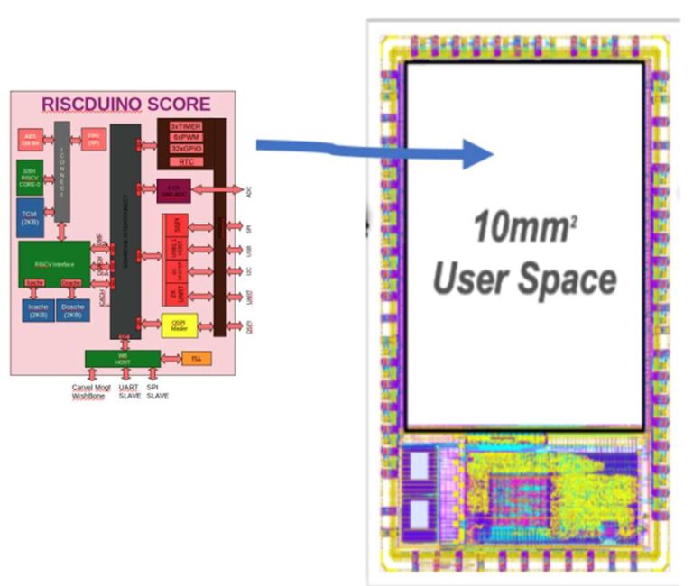
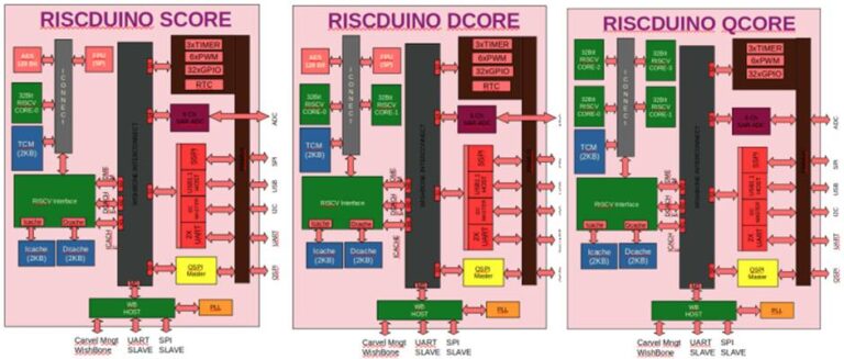
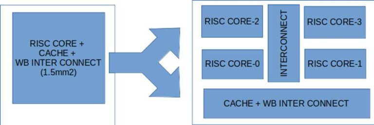
The hierarchical design flow methodology using OpenROAD™ and OpenLane significantly reduces runtime and eases design complexity for the target user area die size (10 mm2) and pre-defined pin constraints of the Caravel GPIO. Dinesh implemented three derivatives of the main RISCduino core: single, dual and quad, as shown in the figure below.
Find details here: https://github.com/dineshannayya/riscduino#readme
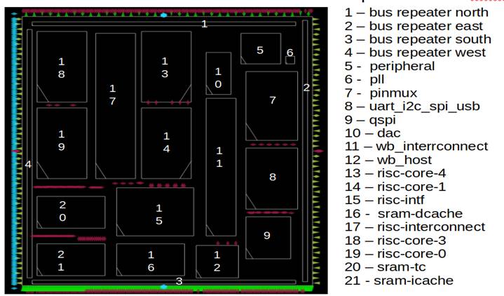
For his last design iteration, Dinesh was able to achieve a significant performance improvement (100Mhz at typical corner) with increasingly dense designs and a high utilization. Shown below are 21 blocks or Macros at the top-level SoC.
This allowed him to focus on good block-level implementations, which after hardening as Macros were easily integrated at top-level. This also vastly simplified top-level routing and timing closure.
Implementation Using a Hierarchical Flow
Dinesh employs a hierarchical instead of a flat design methodology to better manage block-level performance for faster runtimes and better usage of memory. He uses a combination of a top-down approach for design partitioning, time budgeting and top-level placement, and a bottom-up approach to harden Macros, perform SoC integration and achieve final design convergence.
Here are the main steps:
Design Partitioning and Block-level Constraints
- Design partitioning is based on functionality to minimize interconnect signals and combinational logic between the blocks. Here are some guiding rules that Dinesh used:
Rule-1: Too many design components fragment the floorplan, making it difficult to floorplan and close top-level timing. Group smaller and similar components of the functional units into blocks each less than 0.5mm2
- Design partitioning is based on functionality to minimize interconnect signals and combinational logic between the blocks. Here are some guiding rules that Dinesh used:
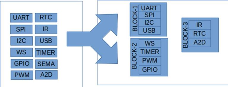
Rule-2: A flat design approach leads to longer RTL-GDSII flow runtime and timing closure challenges at chip level. Logically partition the design into multiple blocks around 0.5mm2 each.
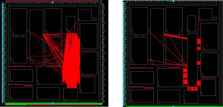
Macro Placement
In this case a manual Macro placement is used to give better pin placement, block-level interconnects and feedthroughs for routing efficiency.
Rule 1: Manual Macro pin placement gives better global routing. Use OpenROAD to preview Macro connectivity and rearrange Macro pin placement.
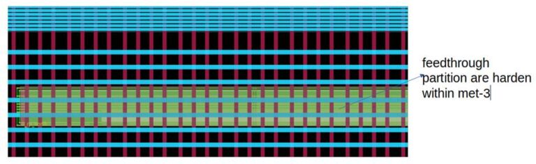
Rule 2: Add Feedthrough partition to connect blocks to top-level i/o for congestion-free routing
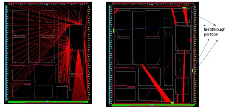
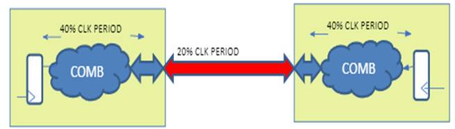
Feedthrough paths are defined from top-level I/O pins into and through the blocks to reduce long routes and congestion. Repeaters are added to these paths to maintain signal strength and avoid max slew and fanout violations.
These feedthrough partitions are manually inserted at 4 corners of the design. The partition I/O signals and position are based on the physical location of the corresponding top-level I/O ports and Macro pins. Finally, these partitions are hardened in met-3, so that they do not block global met-4/met-5 PDN stripes. Timing for feedthrough paths is analyzed by extracting the SPEF parasitics of the paths inside the partition and running timing analysis in OpenLane at top-level.
Time Budgeting and Setting Constraints
Dinesh estimated I/O budgets for each block using a good rule-of-thumb and subsequently re-adjusted the block-level SDC based on top-level hierarchical timing analysis.
Rule-1: Create Block level SDC with I/O Setup delay constraints at Macro ports. Allocate: 60% for external delay with 40% total for block + 20% interconnect. Hold delay constraints:1ns External delay
Rule-2: Run hierarchical timing analysis at top-level; if there are violations, try to re-adjust the I/O timing of the Macro SDC, re-harden it, and re-analyze the top-level timing. This is generally an iterative step until all constraints are met.
Hierarchical Timing Signoff
For MPW2-6 shuttle submissions, Dinesh used his custom top-level scripts using Macro spef + Standard cell .lib to do hierarchical time analysis. An example script is available at:https://github.com/dineshannayya/riscduino/blob/master/sta/scripts/caravel_timing.tcl
Note: Efabless MPW-2 Silicon debug exposed an RCX extraction issue in the hierarchical design and since then the Efabless team revised the tiiming script. From MPW-7 onwards Dinesh used the default timing script. Read this for more information:
https://caravel-user-project.readthedocs.io/en/latest/#running-timing-analysis-on-existing-projects
Flow Summary
Here is a summary of the flow steps:
- Design Partitioning
- Time budgeting and defining initial constraints
- Floorplanning
- Macro placement and feedthroughs
- Fine tuning SDC constraints
- Power network generation
- Clock tree synthesis at top-level
- Balance clock skew
- Add repeaters as needed
- Harden each Macro RTL-GDSII implementation in OpenLane
- Top-level integration
- Hooking up Macros to top-level
- Chip-level signoff
- Load verilog files for all levels of hierarchy
- Load Macro & Top-level SPEF files
- Run top-level, flat timing analysis for all three corner
- Make sure that there are no hold violations in 9 corners –Library (Fast/Typical/Slow) Vs Spef (Max/Nom/Min)
- Analysis the Max timing margin for each clock domain across each corner.
Key Design Strategies to achieve good PPA
Dinesh customizes the flow implementation to leverage many improvements to OpenROAD’s clock tree synthesis (CTS), router (DRT) and power network creation (PDN) to further improve productivity and QoR. Here are some interesting techniques he uses to improve his design to achieve good PPA with the given the flow capabilities:
Better Power management -- Multiple power regions lead to better use of routing resources
Step-1: Macro Power Pitch/Width changed from default 153um/1.6um to 100um/6.2um
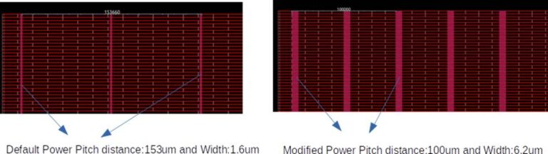
Step-2: Reduce top-level PDN pitch from 153um to 100um and increase width from 1.6um to 6.2um to enable an efficient 9 multi-via hook-up from top-level to Macro.
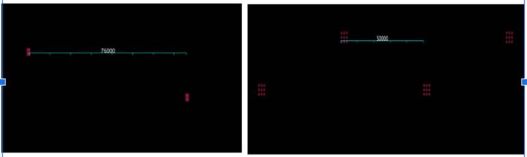
PDN with 2 via vs 4 vias hookups
Now Macros are connected through 9 multi-cut vias compared to 2 vias for better reliability and lower resistance which resulted in lower IR drop
Step-3:Ensure that feedthrough partition is hardened within met-3 so that this will not create a blockage for top-level met-l4 and met-5 power stripes routing.
Since a repeater partition needs distinct power hook-up requirements compared to the rest of the Macros, he defines a separate power-domain for the power connections. Here is the pdn script:
https://github.com/dineshannayya/riscduino/blob/master/openlane/user_project_wrapper/pdn_cfg.tcl
Power grid on side blocks has thicker straps hence less IR drop.
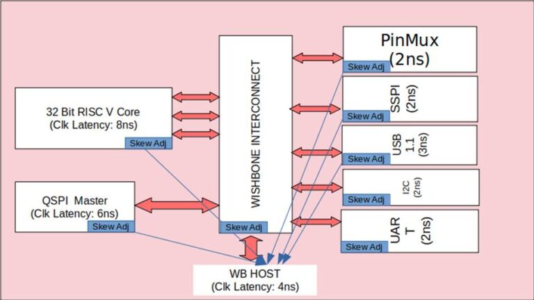
Clock Tree Balancing
Currently, the OpenLane flow does not automatically balance clock skews across the Macros. Shown below is an example where each Macro has a different clock latency. Dinesh defines each Macro with16-tap adjustable clock skew buffers. Each Macro is hardened with skew adjusted to close timing at the top-level Caravel design.
Final Design Results
Using a customized, hierarchical flow, Dinesh was successfully able to meet his design goals. The table below shows the user area utilization for the riscduino_qcore design which has around 150K cells + 48 Kb SRAM (from sky130 pdk) . For the typical timing corner, the RISC-V Arduino core timing performance was met at an fmax of 100Mhz.
|
Block |
Total Cell |
Combo |
Seq |
Utilization |
|
RISC (4 Core) |
94165 |
79675 |
14490 |
45% |
|
QSPI |
9038 |
7525 |
1513 |
42% |
|
UART_I2C_USB_SPI |
11880 |
9011 |
2869 |
42% |
|
WB_HOST |
6511 |
5359 |
1152 |
45% |
|
WB_INTC |
6674 |
5263 |
1411 |
20% |
|
PINMUX |
11923 |
9318 |
1061 |
35% |
|
PERIPHERAL |
5847 |
4786 |
1061 |
42% |
|
BUS-REPEATER |
922 |
922 |
0 |
20% |
|
|
|
|
|
|
|
TOTAL |
146960 |
121859 |
25101 |
|
Final Routed Design
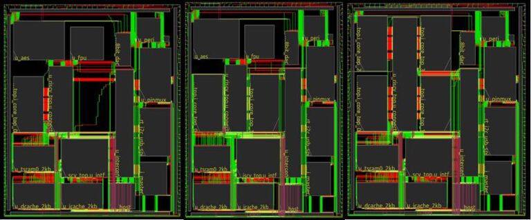
Figure below shows the final routed GDSII for the RISCduino Score, Dcore and QCore designs.
Conclusion
Dinesh summarizes his usage experience of OpenROAD™ and OpenLane as below:
“I highly appreciate the time and effort taken by the OpenROAD team in developing a VLSI design flow based on open-source concepts. Each of the VLSI design stages from RTL-GDSII flow needs specialized technology knowledge and in depth implementation strategy with coordinated effort and strategy. I see a continuous improvement in the OpenLane tool over each MPW shuttle.
I am highly impressed by the OpenROAD team. Response to users in terms of tracking key GitHub issues and overall response time to fix is better than a commercial tool vendor support team. I look forward to a successful commercial tape-out through the OpenLane flow and wish the OpenROAD team the very best for their innovation and mission in OpenEDA flows- in particular in enabling this design flow success as a unix and arduino initiative.
In my technical career I have noticed multiple commercial tool vendors developed an automated RTL to GDS flow and none of these were successful. Main reason for the failure is that every company flow, project & user requirement are unique and each project needs some customization which cannot be easily mapped into a one single RTL to GDS flow. My suggestion to the OpenROAD team is to have clear industry standard handoffs between each stage so that users can effectively use Open-Source EDA tools with commercial tools and Custom Scripts in their commercial projects. I also would like to see missing functionality like Logic Equivalence checking (LEC) and DFT support (JTAG, MBIST, SCAN) added.”
About Dinesh Annayya
 Dinesh is an expert SoC designer and has worked in the VLSI industry for more than 20 years, at companies including Cypress Semiconductor, Centillium and Transwitch. Currently he is working as a design manager in Intel India Bangalore Centre. His design work spans multiple foundries including TSMC, Intel, GlobalFoundries, UMC and SMIC and multiple technology nodes including 180nm, 130nm, 90nm, 65nm, 55nm, 45nm, 22nm and 10nm. He has submitted 28 GH issues that have resulted in critical bug fixes that led to significant enhancements to tool features and quality.
In the future, he plans to extend RISCduino with other add-on chips for advanced functionality and fast interconnectivity interfaces such as QUAD SPI.